
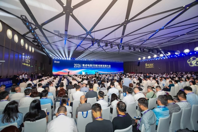
As advanced packaging evolves from "increasing interconnect density" to "system-level integration," reliability challenges expand from the chip level alone to thermal-mechanical coupling across chips, interposers, substrates, solder joints, and packaging materials. On 2026 8, 31, 2026 launched Shenghe Jingwei's advanced packaging R&D platform at the IC (Wuxi) Innovation Development Conference; later that month into early 9, SEMICON Taiwan 2026 highlighted advanced packaging, HBM, Chiplet, and heterogeneous integration as key topics. This signals that 2.5D/3D packaging is accelerating into R&D validation and mass production, where thermal stress, warpage, and temperature cycling reliability are now critical—not just to "make it work," but to ensure "long-term stable operation."
1. Advanced Packaging Enters Accelerated Deployment Phase
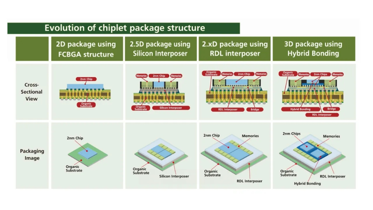
2.5D packaging typically integrates logic chips, HBM, or other functional die side-by-side on an interposer, achieving high-density interconnects through micro-bumps, re-distribution layers (RDL), and TSVs. 3D packaging further stacks chips vertically, shortening interconnect distances via TSVs, micro-bumps, or hybrid bonding to boost bandwidth and integration density.
This architecture is ideal for AI, high-performance computing, and high-bandwidth storage, but it also introduces more materials, more interfaces, and smaller interconnects. The coefficients of thermal expansion (CTE) for silicon, copper, solder, substrates, underfill, mold compounds, and thermal interface materials are not matched, so temperature changes no longer mean just "the chip heats up." Instead, they cause cyclic differential expansion and contraction across the different materials.
II. Why does 2.5D/3D packaging exhibit more pronounced thermo-mechanical coupling issues?
The core reason is straightforward: temperature changes induce thermal strain, and different materials have different coefficients of thermal expansion (CTE). Under linear approximation, thermal strain is expressed as ε_th = α·ΔT, where α is the CTE and ΔT is the temperature difference relative to a reference. When adjacent materials are bonded, they cannot expand or contract freely; thus, CTE mismatch converts into interfacial stress, shear stress, and overall warpage.
For traditional packaging, this issue primarily occurs between the chip, solder joints, and substrate. In a 2.5D/3D structure, deformation is driven by the interposer, micro-bumps, TSVs, HBM stacks, underfill materials, and thinner chips. Additionally, localized hot spots create significant temperature field non-uniformity. Consequently, the same maximum junction temperature does not imply equivalent thermo-mechanical risk.
The 202026 review on advanced packaging clearly states that multi-material stacking and 3D integration inevitably introduce CTE mismatch, potentially leading to thermal stress, warpage, and interconnect failure. Another review on 2.5D/3D chiplet thermal management highlights that high power density creates localized hot spots and non-uniform temperature fields, further impacting long-term reliability.
3. Why does temperature cycling reveal issues better than a single high-temperature exposure?
Many packaged structures remain functional after a single thermal cycle. However, during repeated heating, holding, and cooling cycles, micro-bumps, solder joints, and interfaces are subjected to cyclic loading. Repeated stress in each cycle can induce low-cycle fatigue, interface delamination, creep-fatigue in solder, crack initiation, and propagation.
JEDEC's current JESD22-A104F.01 (2023) is used for thermal cycling tests to evaluate the ability of devices and solder interconnects to withstand thermomechanical stress under alternating high and low temperature extremes. For advanced packaging, testing must go beyond verifying that the chamber temperature reaches the setpoint; it must also monitor the actual sample temperature, temperature differentials, ramp rates, dwell times, and cycle counts.
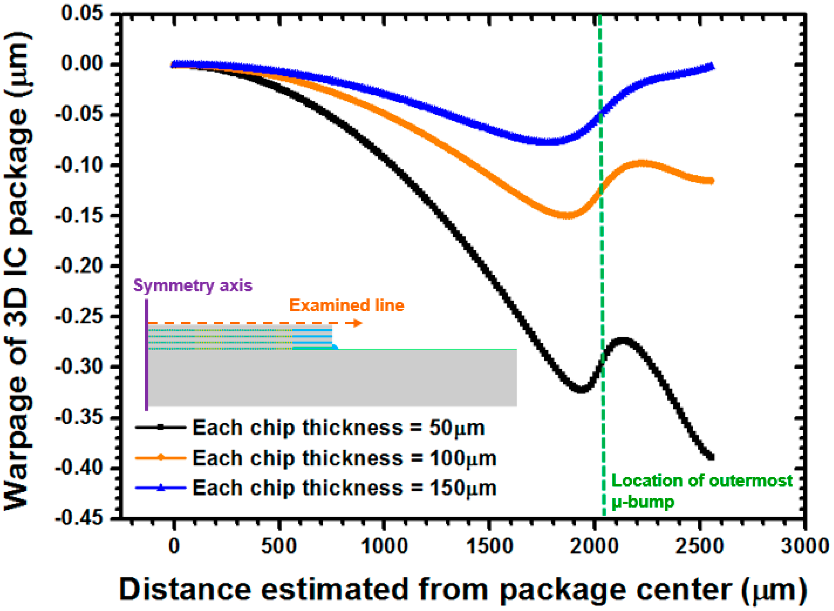
Lee et al. investigated thermal-mechanical reliability of microbumps in ultra-thin stacked 3D-ICs by combining temperature cycling tests with finite element analysis. Results show that chip thickness, underfill elastic modulus, and CTE all affect reliability. This demonstrates that temperature cycling tests not only screen for failures but also guide material and structural design.
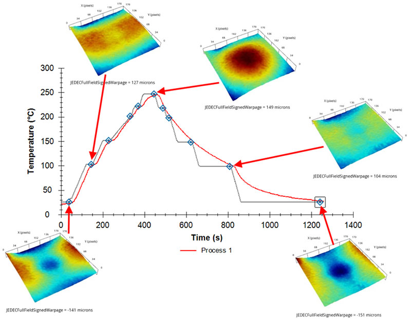
For advanced packaging, the true requirement is not validation at a single temperature point.
For 2.5D/3D packaging R&D, thermal reliability validation should at minimum monitor the following variable categories:
- Temperature Field: Actual temperatures of the chip, HBM, package surface, and critical interfaces, including hotspots and temperature gradients.
- Thermal Cycling: High/Low Temperature Range, Heating/Cooling Rates, Soak Time, Cycle Count, and Actual Sample Temperature Response
- Warpage and Distortion: Out-of-plane deformation during reflow, thermal cycling, and operating temperatures must remain within bonding, mounting, and interconnection tolerances.
- Interface Reliability: Delamination, cracking, and fatigue at interfaces such as TIM, underfill, molding compound, interposer, and microbumps.
- Thermo-mechanical coupling: Stress concentration locations and cyclic cumulative damage under combined temperature variation and CTE mismatch
V. Industry Insights: Reliability validation is shifting earlier, becoming more granular, and increasingly coupled.
Industry trends from 2026 show that advanced packaging is no longer just an upgrade of single-package processes; under the drive of AI/HPC demand, it has become a key path to improving system performance. As Chiplet, HBM, and 2.5D/3D heterogeneous integration accelerate deployment, thermal management, material compatibility, stress control, and long-term reliability must be addressed earlier in the R&D phase—not treated as "end-of-line validation" after product finalization.
This also means the testing methodology itself must evolve: shifting focus from peak temperature alone to full thermal distribution; from single high-temperature exposure to repeated thermal cycling; from isolated thermal performance evaluation to coupled thermo-mechanical-electrical analysis; and from standardized test conditions to validation scenarios tailored to specific package structures, material systems, and actual operating environments.
Reference Materials
- [1] Jiangsu Provincial Department of Industry and Information Technology. 2026Inauguration of the Integrated Circuit (Wuxi) Innovation Development Conference. 2026-09-01.
- [2] SEMI. SEMICON Taiwan 2026 to Serve as the Global Stage Where the Semiconductor Industry Defines What's Next. 2026-06-15.
- [3] SEMI. SEMICON Taiwan 2026: Highlights AI-Driven Manufacturing Transformation. 2026-07-08.
- [4] Advanced Electronic Packaging Technologies: A Comparative Review of Architectures, Applications, and Reliability. Micromachines, 2026, 17(9), 1039.
- [5] Wang Y., et al. Research on the Reliability of Advanced Packaging under Multi-Field Coupling: A Review. Micromachines, 2024, 15(4), 422.
- [6] Virmani D., Chatterjee B. Thermal Management Challenges in 2.5D and 3D Chiplet Integration: A Review of Architecture–Cooling Co-Design. Eng, 2025, 6(12), 373.
- [7] JEDEC JESD22-A104F.01: Temperature Cycling, 2023.
- [8] Lee C.-C. Effect of Wafer-Level Underfill on Microbump Reliability in Ultrathin-Chip Stacking 3D-IC Assembly During Thermal Cycling Tests. Materials, 2017, 10(10), 1220.